Printed Circuit Board

Prodigy’s component divisions supports global customer’s to manufacture custom Printed Circuit Boards (PCB) from its manufacturing centers in China and Taiwan.

Technologies

Rigid PCB
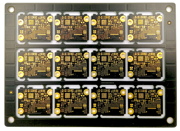
Rigid PCBs are produced with a solid material which prevents them from twisting. Once manufactured they can no longer be modified or folded into shapes. Rigid PCBs are well-known for its high density, high reliability, designable, testability and maintainability. They are also relatively less-cost than other types of PCB, which is one of the reason rigid PCBs are widely considered when producing electronic products.

Layer Count: 1 to 64 Layers
Board Thickness: 0.25mm to 10mm
Dimensions: 1092*660mm (max.)
Final Cu Thickness: Inner 12oz/ outer 12oz (max.)
Line Width/ Space: 3mil/ 3mil (min.)
Drilling Diameter:
Aspect Ratio: 15:1
Impedance Control Tolerance: +/- 8%

Flexible PCB
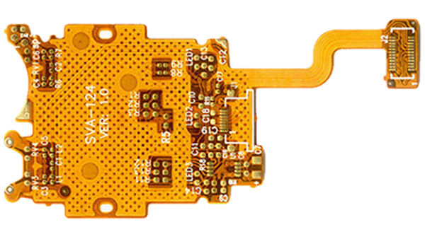
Flexible PCBs offer more options and configurations when assembling electronic circuits. They are manufactured with flexible plastic material which enables the ability to fold over edges and wrap around corners, making them become one of the most important components in today’s most advanced electronic products.

Layer Count: 6L
Board Thickness: min. 0.03mm (1L FPC), tolerance min. +/- 0.03mm
Dimensions: 500*650mm (max.), 10*10mm (min.)
Material: FCCL, stiffener, cover-lay
Final Cu Thickness: 1/3-1oz (iner layer base Cu), 1/3-2oz (outer layer base Cu)
Line Width/ Space: 0.075/ 0.075mm finished Cu 0.5oz inner layer, finished Cu 1oz outer layer
Finished Drilling: CNC drill: min. Ø 0.15, laser drill: min. Ø 0.1mm
Aspect Ratio: laser drill: max. 1.2:1, CNC drill: max. 15:1

Rigid-Flex PCB
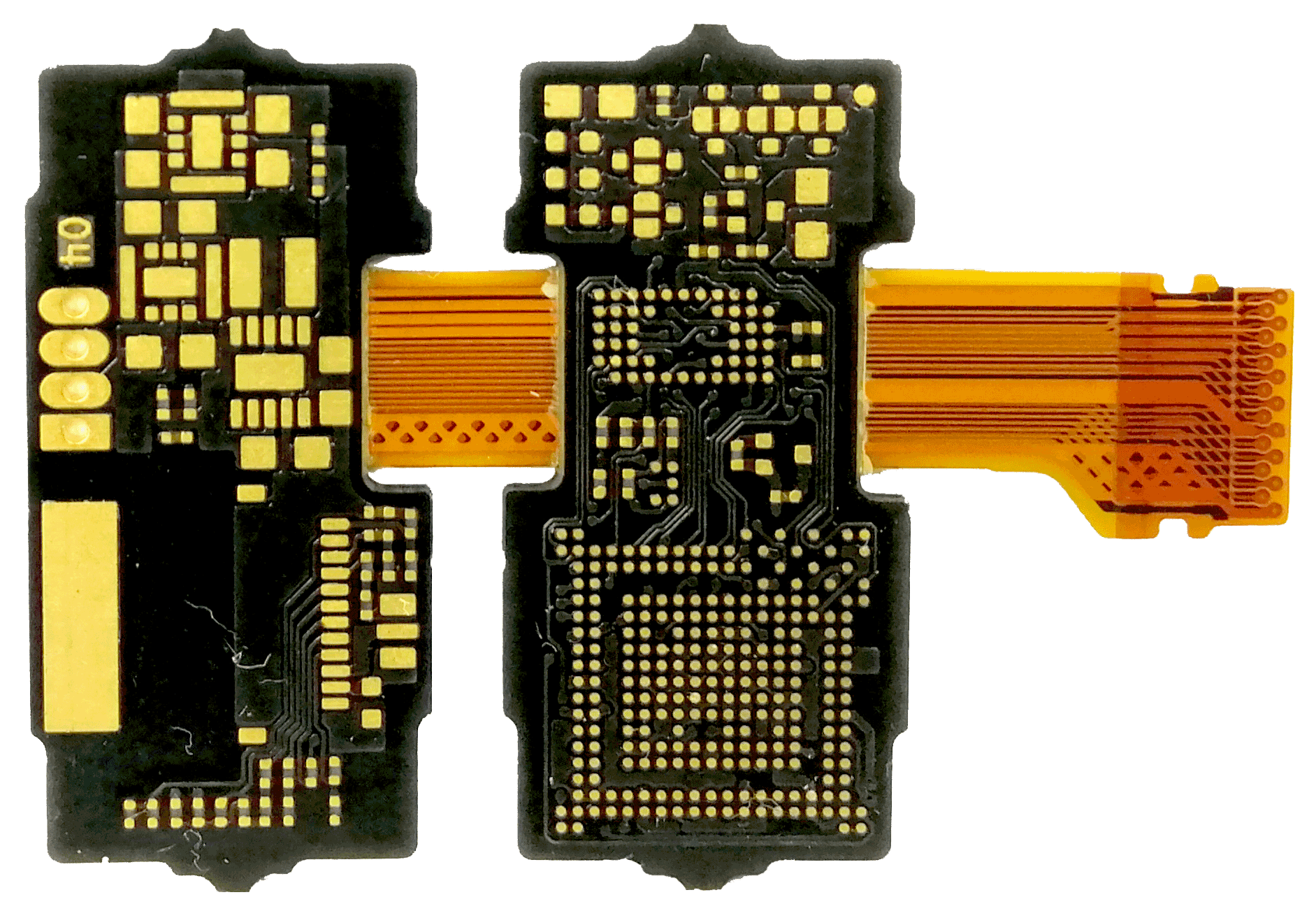
Rigid-Flex PCB is the combination of rigid and flexible board technologies. This allows an application to have a more streamlined design and ability to reduce the overall board size and package weight.

Layer Count: 1 to 64 Layers
Board Thickness: 0.25mm to 10mm
Dimensions: 1092*660mm (max.)
Final Cu Thickness: Inner 12oz/ outer 12oz (max.)
Line Width/ Space: 3mil/ 3mil (min.)
Drilling Diameter:
Aspect Ratio: 15:1
Impedance Control Tolerance: +/- 8%

HDI PCB
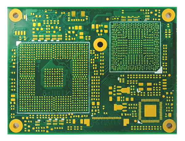
HDI technology enables a PCB to have higher wiring density, which greatly enhances its electrical performance and optimizes overall package weight and dimension of an equipment.

Layer Count: 48L (4+N+4)
Board Thickness: 0.3mm to 8mm (min. to max.)
Dimensions: 250*330mm (max.)
Final Cu Thickness: Inner 12oz/ outer 12oz (max.)
Line Width/ Space: 3
Drilling Diameter:
Max. Aspect Ratio: 1:1

Heavy Copper PCB
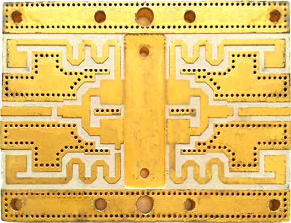
Heavy Copper circuit boards are the core components of household appliances, high-tech products, medical or military equipment, due to the fact of the high durability, good heat dissipating and transferring capabilities.

Layer Count: 1 to 64 Layers
Board Thickness: 0.25mm to 10mm
Dimensions: 1092*660mm (max.)
Final Cu Thickness: Inner 12oz/ outer 12oz (max.)
Line Width/ Space: 3mil/ 3mil (min.)
Drilling Diameter:
Aspect Ratio: 15:1
Impedance Control Tolerance: +/- 8%

Metal Clad PCB
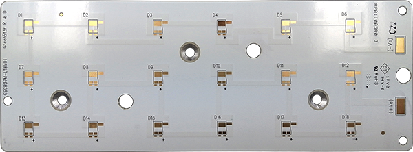
Metal clad PCB is a type of circuit board that consists of metal laminate and electrically insulated layer. Therefore it adds up extra strength and endurance to the product, best for applications with high temperature and pressure involved.

Layer Count: 1 to 64 Layers
Board Thickness: 0.25mm to 10mm
Dimensions: 1092*660mm (max.)
Final Cu Thickness: Inner 12oz/ outer 12oz (max.)
Line Width/ Space: 3mil/ 3mil (min.)
Drilling Diameter:
Aspect Ratio: 15:1
Impedance Control Tolerance: +/- 8%

Materials

Learn More

FAQ

We build single-sided, double-sided and multilayer plated-thru-hole boards. Currently, we are best equipped for prototype, small and medium production quantities on FR4 and high end material. Size and complexity of the boards will determine what our capacity is. We offer solder mask with or without SMOBC, legend silk screening, nickel/gold-plated tabs and CNC scored or routed boards. We specialize in scoring panelization for fast efficient assembly of your bare boards.

Two possible reasons are this would be that you either requested a different quantity or a different delivery. Allowing for nominal increases for the rising prices of material and labor, the price you are quoted should be consistent with previous quotes or orders as long as the quantities and deliveries remain the same. Circuit boards are custom manufactured and the price is very dependent on the quantity being manufactured and the time allowed. Since we have to perform as many steps in the manufacturing process for 1 board as we do for 1000 boards, efficiency dictates that the more product that we can run through the numerous processes required, the more time we save per board. That time saved results in better pricing for larger quantities.

Simply stated, it stands for Solder Mask Over Bare Copper. Traditional solder mask coatings are done over a reflowed tin/lead finish. Although the tin/lead finish is desirable for the pads for better solderability, this tin/lead coating is not necessary for the rest of the circuitry if it is protected by solder mask. The real reason for developing this process was to prevent the wrinkling effect of the tin/lead trapped under the solder mask when it is again reflowed during the assembly operation when the components are soldered with a wave solder machine.

It’s called DFM – Design for manufacturability. This consideration in designing the artwork will save money over and over again during the manufacturer of the bare boards and the assembly of these boards. Contact us for detail.

Keep in mind that the more information you give us, the better the quote will be. Quantity and a fab drawing consisting of outline dimensions, drilling info and any special fab notes. You may simply fill in our quote form with this info or call us for a quick response. You can email this information with Gerber files and we will extract this info but it may delay the quote.

Once we have received the above information, we can usually reply to a quote within 24 hours or less.

We prefer to test your boards but this is an optional process requiring a test fixture charge. You will not pay for this fixture again if the board does not change. The test is a bed of nails netlist test for opens and shorts based on the nets extracted from the Gerber files supplied for the fabrication. Once tested, the boards have been verified to match the Gerber files 100% against opens or shorts.

Most companies have moved away from hard copy artwork these days. The generally accepted method is to transfer electronic (Gerber and HPGL) data by modem or Internet. However modems can sometimes be troublesome with compatibility problems, busy lines and the expense of long distance calls. So increasingly the Internet offers a trouble free, cost effective service. An important point, most PCB manufacturers prefer customers to include the machining details in the form of a drawing within the electronic data package. This enables work to begin immediately – often this item is forgotten.

Basic specification data is often omitted. We need to know finished board thickness, copper weight of inner and outer layer, material, number of layers, dimension, surface finish, silk screen legend color, solder mask color, profile tolerance and ML build if impedance is critical.

The profile of a board should always be referenced to an easily recognized datum. This can either be a component hole or the finger of a gold edge connector. Clear, uncluttered dimensions eliminate any chance of error or confusion. The golden rule must be keep it clear and simple.

All the area not occupied by drilled holes or surface mount pads. It is often difficult to design a board that meets this requirement. When designs are received where silk screen legend encroaches upon the holes or pads a competent manufacturer will have the facility in its front end work stations to clip out the offending text. This obviously needs the customer’s permission and can delay the commencement of production.

This should be considered as 0.1 mm for the production of cost effective boards.

Yes, and it should be remembered that these must be at least 0.3mm larger than the finished hole size to ensure that the drilled hole is adequately surrounded by copper at all stages of manufacture.

This is a most unwise procedure. These isolated tracks will become over plated and will be difficult to cover with solder mask. If the design needs an isolated track then it is advisable to cross hatch the unpopulated area.

As boards are stacked for drilling, the size of the smallest hole determines the drilling stack height. Often via holes are unnecessarily made too small with the effect of increasing drilling costs. For most manufacturers, the smallest via before incurring a cost penalty would be around 0.45mm finished size.

The cost of a blind and buried via board depends upon the quantity of holes between different layers as this will dictate the number of bonding and drilling operations. Typically a 50% increase in price occurs. It is often more cost effective to increase the layer count by 2 layers than move to blind and buried via.

One method is to use a different color resist to the standard green. In particular, boards with red resist are very easy to spot. An alternative method is to print legends with a different silk screen color, white or yellow being standard.

We prefer to receive Gerber data, HPGL, extended Gerber CAM350 (RS274X) or ACAD DWG/DXF, but if you cannot output in these formats, send your design data and we will arrange for it to be post processed.